Behind-the-scenes story of V10 BV-NAND development revealed
Chip wins '3D & NAND Innovation Award' at FMS 2026
Bit density up 58%, power consumption down 25%
HARC etching and wafer bonding breakthroughs key to success
Product targets high-capacity, high-performance storage demand for AI data centers
![Samsung Electronics' 10th-generation V-NAND, the V10 BV-NAND, unveiled by the company as an industry first. [Samsung Electronics]](https://wimg.heraldcorp.com/news/cms/2026/09/01/news-p.v1.20260805.a3bcc5c7df4e41eda5ed3eabb9179484_P1.jpg)
Samsung Electronics has shared the story behind the development of its V10 (10th-generation) BV (Bonding Vertical)-NAND, which the company unveiled earlier this month at FMS (Future of Memory and Storage) 2026 in the United States. The V10 BV-NAND is the company's latest 3D NAND flash memory chip, featuring an ultra-high-stacking structure of more than 400 layers.
Developing a product with no precedent required overcoming physical limits. Samsung said the challenge was met through a next-generation chip architecture optimized for BV-NAND, with hundreds of engineers combining high aspect ratio contact, or HARC, etching and wafer bonding processes into a single integrated workflow.
As the AI inference era takes hold, the importance of high-capacity NAND has grown more than ever. Demand for storage has surged as large language models store KV cache — the data generated through conversations with users. The V10 BV-NAND is designed to meet that growing storage demand with high performance and low power consumption.
According to an interview published Monday on Samsung Electronics' semiconductor newsroom, the company set out to develop the V10 NAND with the simultaneous goals of high density, high performance and low power consumption. The rapid growth in data generated and processed by AI systems has driven demand for greater capacity and higher I/O bandwidth.
"From the planning stage, V10 was never just about stacking more layers or increasing capacity," said Kim Byung-hee, a product lead on the project. "A key goal was to provide NAND that can handle expanding AI workloads not only in data centers but across a wide range of applications, including PCs, mobile devices and edge AI."
The V10 stacks more than 400 layers on a V-NAND structure using 3D bonding technology. That architecture delivers a bit density — the number of bits stored per unit area — more than 58 percent higher than the previous generation. It also offers I/O speeds exceeding 4.8 Gbps, a performance improvement of more than 33 percent over its predecessor, while cutting power consumption by more than 25 percent.
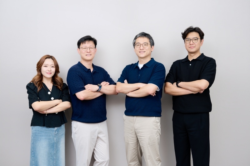
The technical difficulty was equally formidable. The development team described the process as one of overcoming physical limits.
"To achieve the ultimate reduction in chip size, we accomplished a 'full capping' design that perfectly aligns the lower peripheral circuit with the upper cell size," said Park Sang-su, a product lead. "At the same time, we worked with the research division to maximize process capabilities and minimize transistor size."
Samsung overcame technical barriers through innovations in the etching process and wafer bonding. As the number of stacked layers increases, pressure builds on the thin films in the stack, causing wafer warpage. Engineers across eight process disciplines pooled their ideas to introduce new processes and push past equipment limitations.
"HARC merge and wafer bonding — core V-NAND technologies — involve combining what were previously independently developed module processes into one, and merging two separately fabricated wafers into a single unit," said Jeong Da-un, a product lead. "Because we had to understand the work of those around us and solve problems together, it required a great deal of cross-departmental communication and collaboration."
The three-stack-based HARC merge technology applied in the V10 is an advanced stacking technique that divides V-NAND cells into three layers and connects them vertically. As layer counts rise, the depth to which channel holes — which penetrate the data storage cells — can be etched becomes increasingly critical. That is why HARC etching processes continue to grow more sophisticated.
Wafer bonding, in which cells and peripheral circuits are fabricated independently on separate wafers and then joined, also contributed to high performance and low power consumption by maximizing the performance of peripheral devices.
The V10 won the "3D & NAND Innovation Award" at FMS 2026, held earlier this month in Santa Clara, California, in recognition of its technical achievements. Samsung Electronics expects the V10 to address demand for high-capacity, high-performance storage in AI data centers.
"As AI advances, the volume of data that must be processed and stored is expected to continue growing rapidly," said Shin Ji-yeon, a team lead on the project. "The technological innovations in V10 are meaningful because they simultaneously improve the capacity, performance and power efficiency required by AI infrastructure, delivering real value to customers."

jeongwan@heraldcorp.com