Intel foundry under consideration for 7th-gen HBM base die
Base die is the controller chip at the bottom of HBM stacks
Move aims to build multi-vendor supply chain
Diversification would expand customer options and pricing leverage
Intel's advanced EMIB packaging also being tested
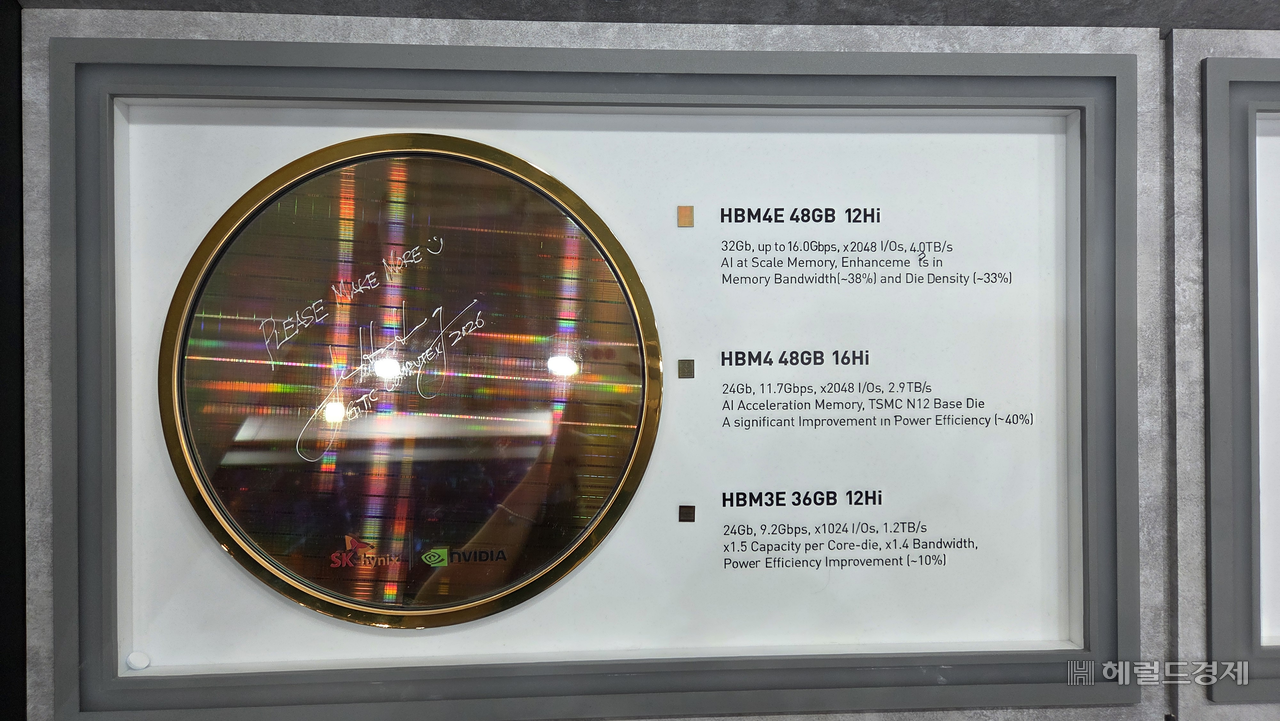
SK hynix is moving to diversify the supply of base dies — the controller chips at the foundation of high-bandwidth memory stacks — as demand for its HBM products continues to grow.
The company is considering entrusting Intel's foundry with base die production starting with HBM4E, its seventh-generation HBM, sources said. Until now, SK hynix has relied entirely on TSMC for base die manufacturing.
Industry sources said Monday that SK hynix is pursuing cooperation with Intel — alongside TSMC — for the base dies used in HBM4E, potentially as early as that product generation. Some analysts say the move is designed to build a multi-vendor supply structure, diversify a supply chain currently concentrated at TSMC, and strengthen SK hynix's pricing leverage in negotiations.
The base die sits at the bottom of an HBM stack, supporting and controlling the entire structure, and is also known as a logic die. It handles the high-speed interface connecting external processors — such as GPUs and CPUs — with the HBM memory chips above.
SK hynix produced base dies using its own process through HBM3E. As HBM generations advanced, however, the logic functions and performance requirements of the base die grew increasingly demanding, prompting the company to begin working with TSMC on base die production starting with HBM4. The HBM4 now in mass production uses a base die manufactured on TSMC's 12-nanometer-class process.
The cost burden of the base die is a central concern. For HBM4, TSMC's base die costs three to four times more than the core dies — the DRAM chips stacked above the base die that store data directly — which SK hynix produces on its own 10-nanometer-class fifth-generation (1b) process, industry sources say. That cost burden is expected to grow further with HBM4E. Because HBM sales rely heavily on long-term supply agreements, passing foundry cost increases directly on to product prices is not straightforward.
If Intel joins the base die supply chain, SK hynix would gain broader options on both cost and supply stability, industry observers say.
The move is also seen as a strategic decision to reduce the company's long-term dependence on a TSMC-concentrated supply chain. As custom HBM — where base die designs are tailored to the AI accelerator architectures and performance requirements of individual customers — grows in importance from HBM4 onward, SK hynix needs to expand its options for working with a wider range of AI chip companies beyond any single customer or foundry ecosystem.
There is also speculation that future cooperation with Intel could extend beyond base die production into advanced packaging. At Hot Chips, a high-performance semiconductor and computing architecture conference held in Silicon Valley, Lee Jae-sik, vice president of package engineering at SK hynix America, said the company is comparing and analyzing major advanced packaging approaches, including TSMC's CoWoS-S and CoWoS-L as well as Intel's EMIB.
go@heraldcorp.com
jeongwan@heraldcorp.com