Groundbreaking held at Asan campus for advanced packaging fab
Line 5 to produce HBM4E by 2028, with 6 trillion won committed
Lee Jae-yong: 'Barren hill will become the heart of AI semiconductors'
Display, battery and substrate affiliates join the push
Samsung eyes Chungcheong region as strategic hub for AI materials and components
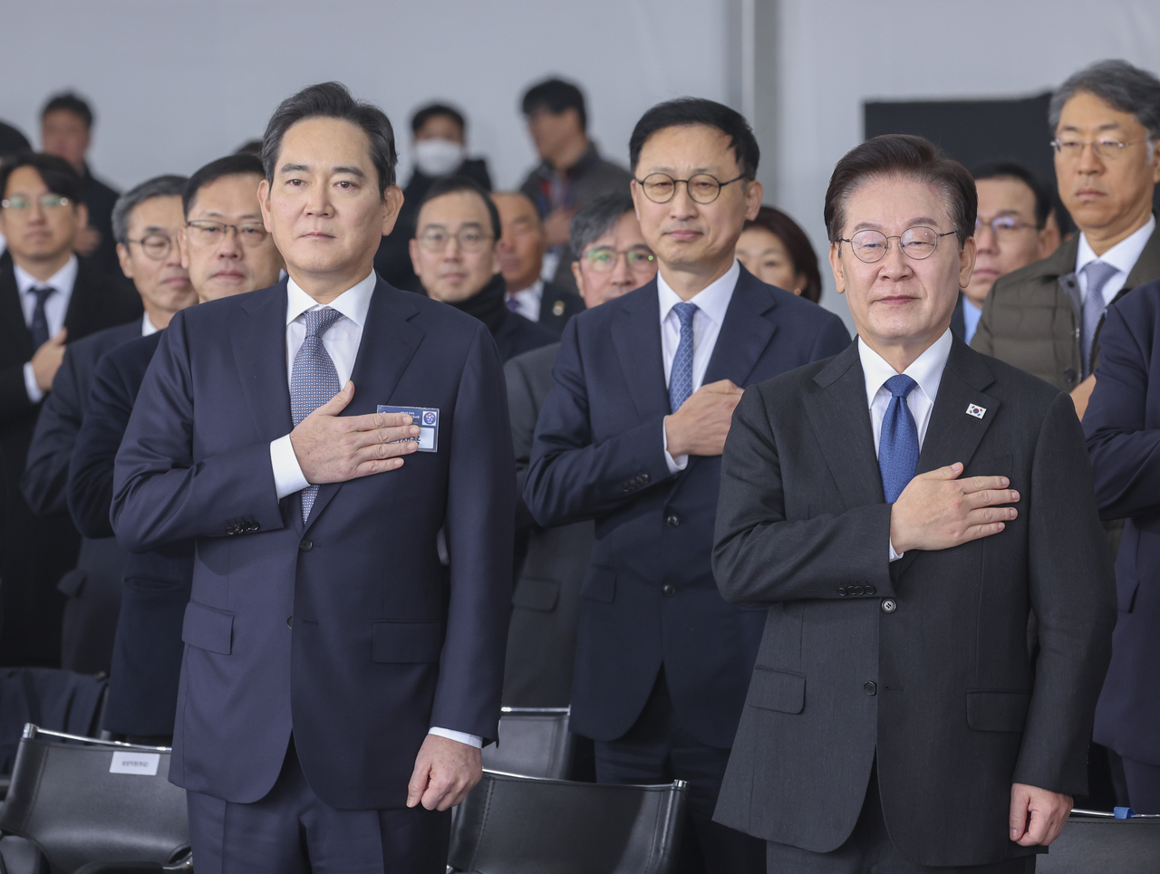
The first project under South Korea's "Three Great Leap Mega Projects" initiative has broken ground at Samsung Electronics' Onyang campus semiconductor complex in Asan, South Chungcheong Province.
Samsung Electronics has chosen the Chungcheong region as its strategic base for strengthening advanced packaging capabilities — a key battleground in the semiconductor industry as the AI era accelerates — and formally launched construction Thursday.
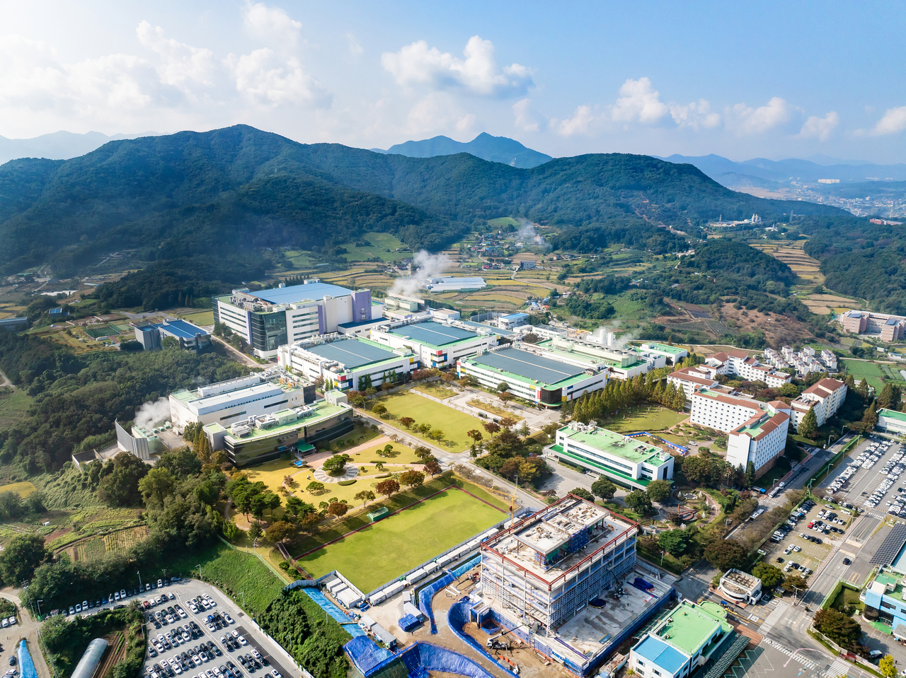
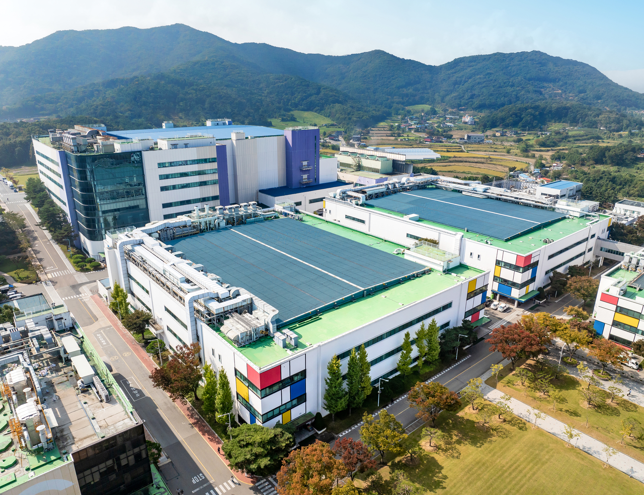
The Onyang campus, established in 1991, has long handled the assembly and testing of general-purpose semiconductors. The new investment will transform it into an advanced packaging hub for high-performance AI chips, including HBM.
Samsung Electronics Chairman Lee Jae-yong, speaking at the groundbreaking ceremony at the Onyang campus Thursday morning, said the site would undergo a fundamental transformation. "This place, which centered on the simple assembly and testing of general semiconductors, will become a state-of-the-art HBM base — the heart of AI semiconductors," he said.
Beyond the semiconductor packaging expansion, Samsung plans to scale up next-generation display production lines in Asan, battery lines in Cheonan and AI server package substrate lines in Sejong, building out the Chungcheong region as a strategic production hub for core AI-era materials and components.
6 trillion won for advanced packaging fab — HBM4E production at Onyang from 2028
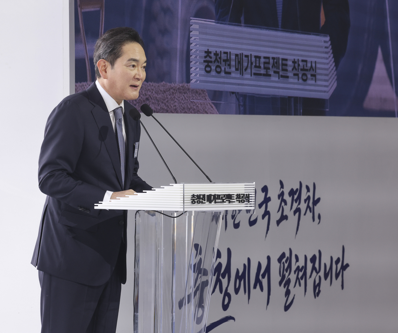
The ceremony drew Samsung Electronics' top leadership, including Chairman Lee, Device Solutions Division Vice Chairman Jeon Young-hyun, management strategy chief Kim Yong-kwan, Samsung Electro-Mechanics President Jang Deok-hyeon, Samsung SDI President Choi Ju-seon and Samsung Display President Lee Cheong.
Samsung Electronics moved up construction of Onyang Line 5 by one year from its original schedule to meet surging demand for AI server memory. Foundational work on the line is already underway, with a target start of operations in June 2028. The project carries an investment of 6 trillion won ($4.49 billion).
The new three-story fab will feature a clean room spanning 31,020 square meters and is set to begin full-scale production of seventh-generation HBM4E and other advanced chips. Samsung Electronics plans to invest a total of 60 trillion won in the Chungcheong region, including Onyang Line 5.
Lee reflected on the campus's transformation. "Forty years ago, all you could see here were barren hills and unpaved roads," he said. "Now it has become a state-of-the-art factory that assembles and tests semiconductors — the rice of industry — through to final completion."
Lee added that Samsung would press ahead with mega projects in the Honam and Yeongnam regions as well as Chungcheong. "With an even greater sense of responsibility, we will actively pursue these projects to write an irreplaceable success story for South Korea," he said.
Advanced packaging: the next frontier in semiconductors
DS Division Vice Chairman Jeon laid out an ambitious vision at Thursday's event. "We will strengthen the semiconductor production base linking Onyang and Cheonan and develop the Chungcheong region into the world's foremost advanced packaging hub," he said.
Samsung Electronics currently operates packaging factories in both Onyang and Cheonan. The Onyang campus marks its 35th year of operation this year since its establishment in 1991, serving as the final gateway in the production chain — handling semiconductor assembly, testing and shipment.
Advanced packaging, the technology Samsung has now committed to expanding, is widely regarded as critical to improving the performance of AI semiconductors. The process involves placing chips side by side or stacking them vertically into a finished product. It constitutes the back-end stage — the final step in the semiconductor manufacturing process.
As the front-end process of etching fine circuits onto wafers approaches its physical limits, back-end packaging has grown in importance as an alternative path to performance gains — combining or stacking multiple chips such as CPUs, GPUs and HBM into a single unit.
Earlier, on Nov. 1 — Samsung Electronics' 57th founding anniversary — Chairman Lee visited the Advanced Packaging Lab in Yokohama, Japan, the company's advanced semiconductor packaging research center, signaling his close attention to next-generation packaging component technologies that will shape Samsung's future competitiveness.
Display, battery and substrates: building a materials and components hub
Beyond advanced semiconductor packaging, Samsung plans to pour large-scale investment into the Chungcheong region across future growth drivers — including cutting-edge displays, next-generation batteries and AI server package substrates.
At a public briefing on the Chungcheong advanced industry development vision held in July, Samsung announced plans to invest about 140 trillion won in the region to develop it into a center of excellence for materials and components.
Samsung Display broke ground last month on its new A7 line within the second complex of its Asan campus — a three-story structure spanning 561,000 square meters. The line targets mass production from the second half of 2029, covering high-value OLED panels for foldable devices, laptops and tablets, as well as extended reality, automotive, humanoid robot and wearable applications.
Samsung Electro-Mechanics also began last month building high-performance AI server package substrate production facilities at its Sejong campus, committing about 4.03 trillion won to the project. The new fab will rise four stories with a total floor area of 99,000 square meters. To meet supply requests from global big-tech customers, the company has compressed the construction timeline as much as possible, targeting mass production by September 2028.
Samsung Electro-Mechanics, which has planned a total investment of 8 trillion won at the Sejong campus, signaled Thursday that it intends to go further. "We will secure additional land nearby and proceed with an investment on a larger scale than originally planned," the company said.
Samsung SDI is investing about 9 trillion won at its Cheonan campus to build a mother line for validating next-generation battery technologies. Construction was completed in July last year and equipment began operating in November of that year. Additional equipment is currently being brought in.
joze@heraldcorp.com