Permit process cut from 4.5 years to 21 months
50 million tons of earth moved, land compensation 99% complete
Water, power and 8-lane road network to serve complex
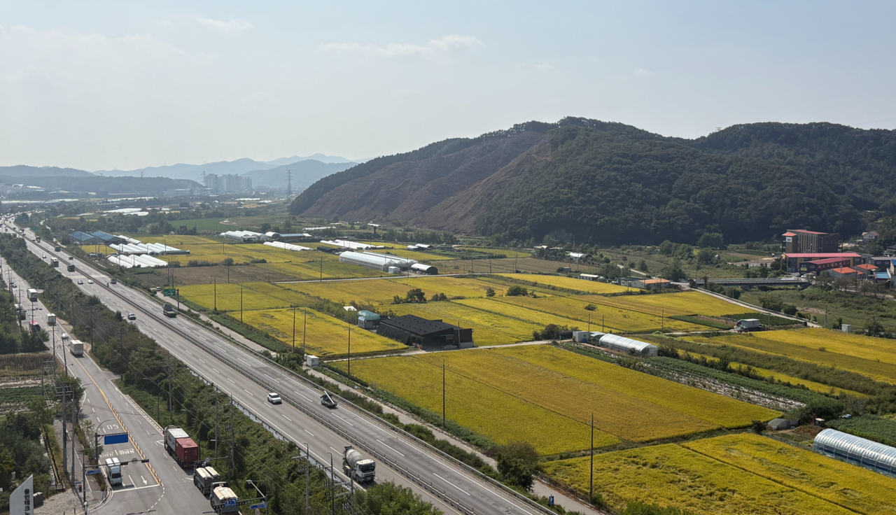
Standing on the rooftop of a building inside the Deokseong general industrial complex in Cheoin-gu, Yongin, Gyeonggi Province on Wednesday, a vast expanse of land designated for the Yongin semiconductor national industrial complex stretched into view. Alongside Dalbongsan — a hill where logging has already begun, exposing red earth — National Route 45 and low-lying farmland were visible. The roughly 4-kilometer-wide, 2-kilometer-deep site is slated to become a key semiconductor hub within a few years.
The Yongin national industrial complex will concentrate six semiconductor fabs, three power generation facilities, an industrial gas supply facility, and a materials, components and equipment zone across approximately 7.78 million square meters in Cheoin-gu. Samsung Electronics' Pyeongtaek campus and its Giheung and Hwaseong campuses, along with SK Group's Yongin general industrial complex, are all located within 15 kilometers of the site.
The complex is also the designated Greater Seoul semiconductor production hub under the government's three major megaprojects announced in June. As global chipmakers race to expand their production bases, the government has said it will fast-track development of the Yongin national complex to strengthen the country's domestic semiconductor manufacturing foundation.
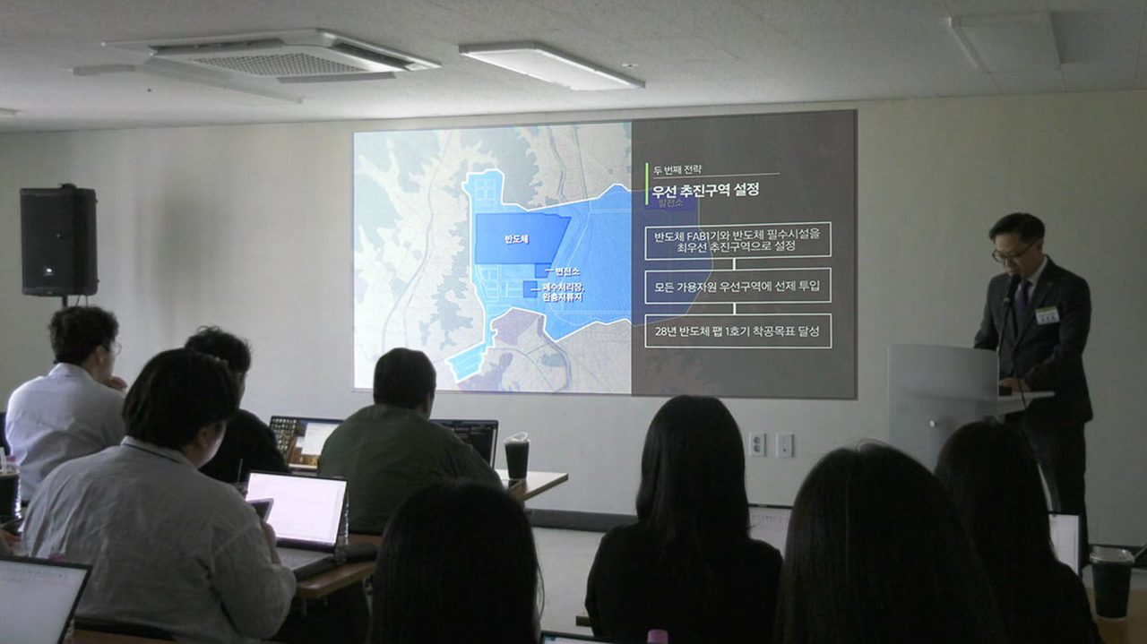
Korea Land and Housing Corporation (LH) is accelerating work on the complex with a target of breaking ground on the first fab in 2028. A Daewoo Engineering & Construction-led consortium was selected as the contractor for the first construction zone — covering 3.45 million square meters and including the site for the first fab. The estimated construction cost is 1.09 trillion won ($801 million). LH plans to sign the construction contract in mid-October and begin work on the priority zone.
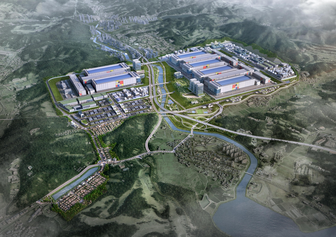
Conditions on the ground in the early stages of the project were far from easy. The site is ringed by steep hills, and the volume of soil and rock that had to be removed reached approximately 50 million tons — six times the fill used to reclaim Yeouido. Compensation had to be arranged for 3,864 parcels of land, an area comparable in scale to the Pangyo new town. The relocation of 401 homes and 231 households also had to be completed first.
That is precisely why LH has made speed its top priority. After the site was announced as a candidate in March 2023, LH filed for industrial complex plan approval in April 2024 and received it eight months later following consultations with relevant agencies.
"We resolved the water-source protection zone regulations that had restricted factory construction by signing a co-prosperity agreement with the central government, local authorities and Samsung Electronics," an LH official at the Yongin project headquarters said. "We also used a pre-consultation system to complete the environmental impact assessment in just 13 days — a process that normally takes years." The entire process from preliminary feasibility study to industrial complex plan approval typically takes four and a half years; for the Yongin complex, it was completed in one year and nine months — more than half the usual time.
Land compensation was also handled swiftly. A public-private consultative body was formed from the outset to identify residents' needs and draw up relocation plans. A compensation plan was announced in June last year, and negotiated compensation began in December of the same year. Compensation procedures have now been completed or initiated for 99 percent of privately owned land — 43 percent through negotiated acquisition and 56 percent through compulsory purchase applications. "A business relocation zone of 495,000 square meters has been planned so that existing companies can continue operating without any interruption, along with a public housing district of 2.28 million square meters adjacent to the complex in Yongin Idong," an LH official said.
On top of that, LH designated the Zone 2 industrial site — where two Samsung Electronics fabs will be built — and the power plant site that will supply electricity in the early stages as priority areas, concentrating project and compensation resources there. Stages that could be run in parallel — design, procurement and preliminary construction — were pushed forward simultaneously to significantly compress the overall schedule.
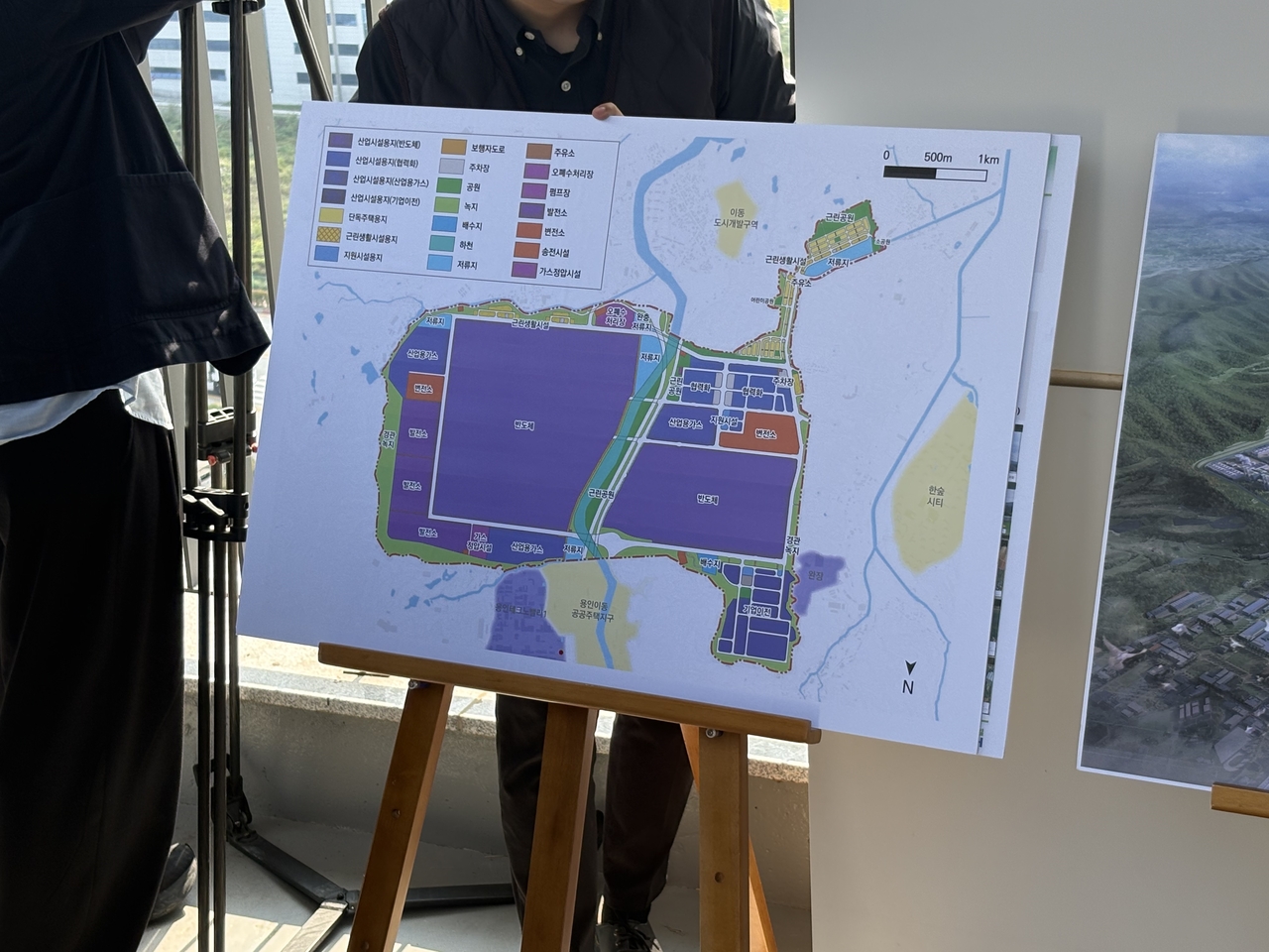
Building semiconductor factories requires enormous infrastructure. Korea Water Resources Corporation will supply approximately 764,000 tons of industrial water per day. Of that, 310,000 tons will be secured first through the Greater Seoul metropolitan water supply system, with an additional 454,000 tons to come from a new intake facility to be built upstream of Paldang Dam. Power will be secured through a new LNG power plant to be built inside the complex.
The road network is also being reconfigured to serve the complex. National Route 45, which currently runs through the project site, will be rerouted to avoid sections that overlap with fab sites and widened to eight lanes. The complex will connect to nearby expressways via four road routes, including National Route 45, and two access facilities.
Once full construction begins, the pace will be stepped up through increased blasting and the addition of access roads for equipment movement. Safety risks that grow with the faster pace will be managed proactively using AI and advanced robotics — quadruped robots and autonomous drones will be deployed to monitor the large-scale construction site. Preliminary work, including logging and cultural heritage surveys, began at the site in September.
A visit Wednesday afternoon to Samsung Electronics' Pyeongtaek campus in Godeok-dong, Pyeongtaek, offered a preview of the semiconductor production facilities that will eventually rise at the Yongin complex. Inside the P1 production line, wafer carriers moved ceaselessly along multi-tiered overhead rail systems installed near the ceiling.
The P1 line at Samsung Electronics' Pyeongtaek campus is a massive facility stretching 518 meters in length. The fabs planned for the Yongin complex will be even larger. "The semiconductor factory at Yongin will measure 638 meters wide, 211 meters deep and 120 meters tall," an LH official said. "That is far longer than Lotte Tower in Jamsil, the tallest building in the country at 555 meters." The official added that it will house the world's largest semiconductor line.
"The biggest priority in the global semiconductor market right now is building production bases quickly," LH President Lee Seong-hun said. "We will manage rigorously to ensure that our acceleration measures are carried out effectively on the ground, and we will do our utmost to complete the project on schedule through active communication with the government and tenant companies."
shy@heraldcorp.com
hss@heraldcorp.com