Aims to secure both product performance and cost competitiveness
Also weighing entry into ASML-linked 12-inch photomask consortium
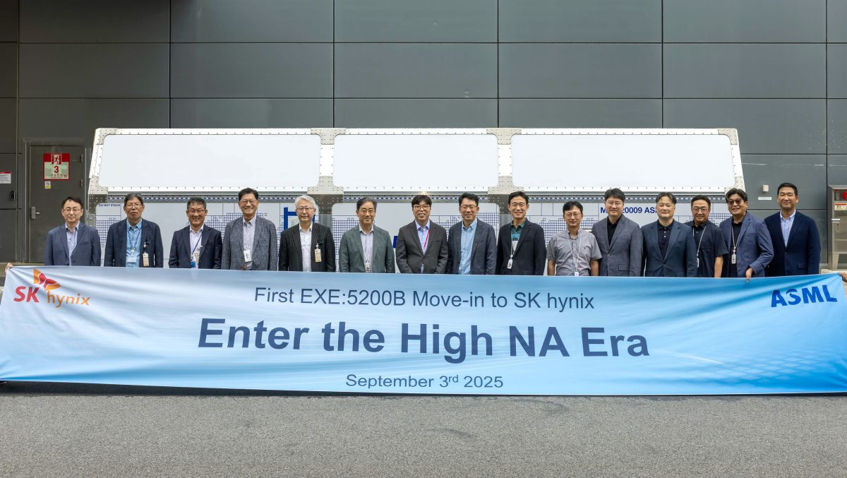
SK hynix said it plans to adopt High-NA EUV, ASML's next-generation lithography equipment, for its DRAM process and begin mass production by 2028. The company is also considering joining the Large Size Mask Consortium led by TSMC.
According to Reuters, SK hynix said in a statement Wednesday that it is reviewing participation in a consortium related to the introduction of 12-inch photomasks.
The company added that it aims to apply the High-NA EUV process to DRAM mass production by 2028.
High-NA EUV can produce finer circuit patterns than conventional EUV equipment.
While conventional EUV equipment has a numerical aperture of 0.33, High-NA EUV raises that figure to 0.55, allowing for more precise circuit formation. This is expected to lift both product performance and productivity to a new level.
SK hynix first introduced EUV technology in 2021 for mass production of its 10-nanometer-class fourth-generation (1a) DRAM and has since expanded its use across more advanced DRAM products.
By adopting High-NA EUV, SK hynix plans to simplify its existing EUV process and speed up the development of next-generation memory chips, securing both product performance and cost competitiveness at the same time.
SK hynix is also considering joining the consortium seeking to shift the industry standard to 12-inch photomasks.
ASML and other global equipment makers have been running a consultative body to move from the 6-inch photomasks traditionally used in lithography processes to 12-inch photomasks. Samsung Electronics is also part of the group.
Samsung Electronics also said the same day that it plans to introduce High-NA EUV technology for the manufacturing of advanced DRAM memory chips by 2028.
go@heraldcorp.com