Samsung Electronics chief inspects Yokohama research hub, eyes technology to boost AI chip performance
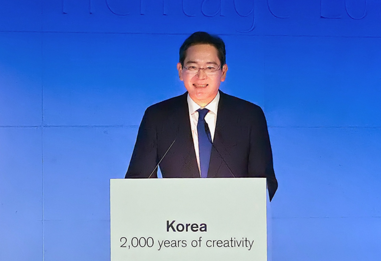
Samsung Electronics Executive Chairman Lee Jae-yong visited the company's advanced semiconductor packaging research hub in Yokohama, Japan, to review the state of technology development there. The visit signals Lee's determination to sharpen Samsung's technological edge by deepening ties with Japanese suppliers of semiconductor materials, components and equipment — partnerships that have grown more critical as advanced packaging emerges as a key battleground in AI chip performance.
Samsung Electronics said Sunday that Lee toured the Advanced Package Lab, or APL, the company's packaging research base in Japan. The visit came roughly two months after the facility formally opened on Sept. 8.
The APL is a semiconductor packaging research and development center established in Yokohama, Kanagawa Prefecture. Samsung announced plans to build it in 2023 and began R&D operations in September. The lab is designed to combine Japanese expertise in semiconductor materials, components and equipment with Samsung's own memory chip and foundry capabilities to secure a competitive edge in next-generation AI semiconductors.
Packaging technology protects semiconductor chips from physical damage and connects them to other components. In advanced AI semiconductors, it also plays a critical role in bundling together GPUs — which handle massive computational workloads — with HBM chips that feed them data, boosting overall performance.
How quickly data moves between chips, and how much power consumption and heat generation can be reduced, all hinge on packaging technology, making it a decisive factor in AI chip competitiveness.
Lee's visit focused on securing advanced packaging technology and exploring ways to strengthen collaboration with Japanese materials and equipment suppliers that underpin that effort.
Japan is home to many companies with world-class expertise in semiconductor materials and equipment. Samsung plans to accelerate next-generation packaging development by integrating Japanese materials and equipment technology with its own semiconductor design and manufacturing capabilities.
The APL serves as a research collaboration hub connecting those two sides. It develops and validates the materials and process technology needed for advanced packaging, and conducts research into bonding techniques for precision chip interconnection as well as next-generation processes and materials such as glass substrates. The lab is also expanding its scope to cover chip placement and interconnect architectures aimed at achieving low-power, high-performance AI semiconductors.
Samsung established the APL in Yokohama in 2023 and has been building out its research infrastructure with an investment of 40 billion yen ($254 million) over five years starting in 2024. The company has received a total of 22.5 billion yen in support from the Japanese government and the city of Yokohama. Yokohama's proximity to Tokyo and its concentration of universities and research institutions make it well suited for recruiting specialized talent.
Samsung said the area's cluster of materials and equipment companies focused on advanced packaging also makes it ideal for joint research and technology collaboration. The opening ceremony held in September was attended by representatives from major Japanese semiconductor suppliers, including Tokyo Electron and Ibiden.
Samsung plans to expand its local research workforce and strengthen ties with Japanese industry, academia and research institutions, with the goal of developing the APL into a global R&D hub for next-generation packaging technology.
Lee has been making rounds at semiconductor facilities at home and abroad, focusing on assessing technological competitiveness to maintain Samsung's lead in the industry. In June, Lee visited the company's Cheonan plant in South Chungcheong Province, which handles back-end processes and advanced packaging for Samsung's HBM chips.
park.jiyeong@heraldcorp.com