Kumamoto Prefecture's hands-on administrative support for TSMC
'Silicon Saxony' built since 1961 shows why local commitment matters
Rep. Jung Jin-wook: 'Livability is an urgent task'
Ex-Samsung executive Chung Eun-seung: 'We will bring these lessons home'
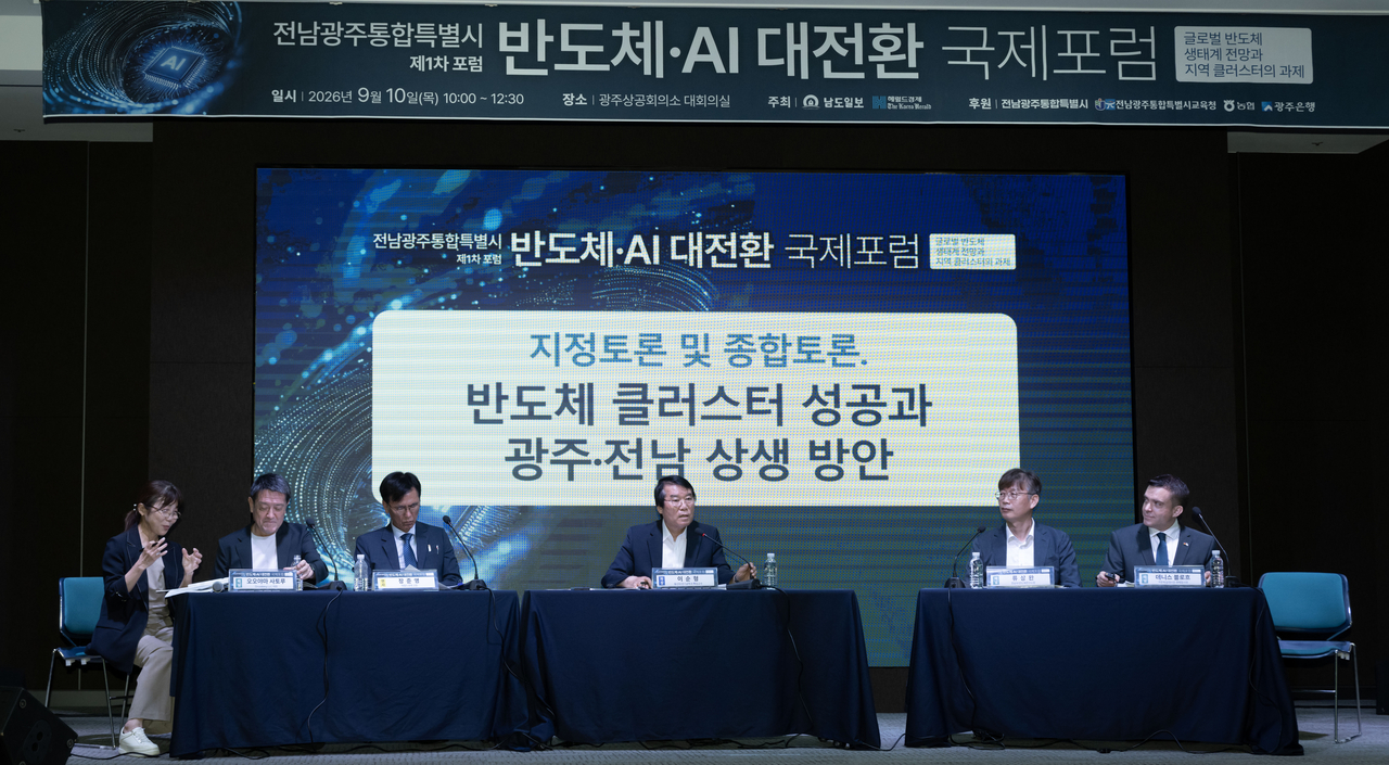
Global semiconductor experts said Gwangju and South Jeolla Province should study Japan's Kumamoto Prefecture TSMC joint venture and Germany's "Silicon Saxony" model to succeed in building the region's semiconductor cluster. National and local governments need to build tailored infrastructure to encourage corporate investment, they said.
Speakers also called for a longer-term view of the cluster development plan. Samsung Electronics and SK hynix currently plan to build four fabs (semiconductor production facilities), but investment should be prepared preemptively given the possibility that the number could grow further, the experts said.
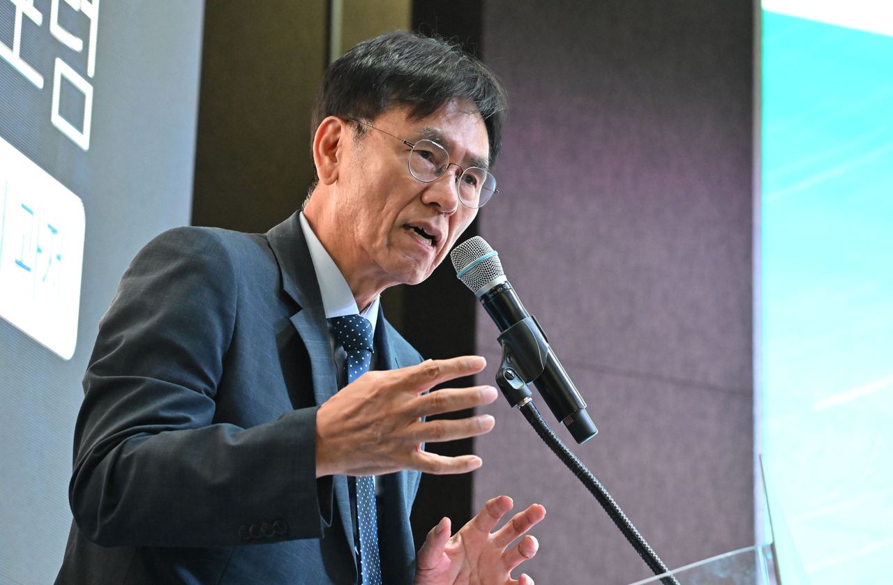
Jang Jun-young, an advisor at The Herald Business, examined how TSMC teamed up with Sony and Toyota Motor to swiftly build a factory, in a presentation titled "A 27-Month Case Study of Kumamoto Prefecture's Semiconductor Cluster Development."
TSMC, the world's largest foundry, established Japan Advanced Semiconductor Manufacturing (JASM) in 2021 and began construction of a factory in Kumamoto Prefecture. It completed the first factory in 2024, which now produces 12- to 28-nanometer semiconductors. A second factory, targeted for completion in 2028, is also under construction and is set to mass-produce cutting-edge 3-nanometer chips.
Jang first explained the background of TSMC's investment in Kumamoto. "TSMC had a long-standing business relationship with Sony, and Sony played a role in attracting TSMC," he said. "The fact that the company itself led the project from the early stages of investment was behind the speedy decision-making."
"Because the company took the lead, the factory could be completed in under three years," Jang said. "The central government provided funding, and Kumamoto Prefecture provided the services companies needed as they carried out the project."
After TSMC announced its investment plan following the establishment of the joint venture, Kumamoto Prefecture unveiled its "Kumamoto Semiconductor Industry Promotion Vision" and formed a dedicated organization that held six review meetings — one every six months — to provide administrative support. Thanks to that hands-on backing, construction of the second factory is also expected to proceed without a hitch.
Jang also stressed the need for policies favoring local companies that already know the region well. "At the time, the central government required that more than 50 percent of investment be spent on companies within Kumamoto Prefecture," he said. "Honam also has many general construction companies, so more than 50 percent of the work should go to Honam-region firms to help speed up the project."
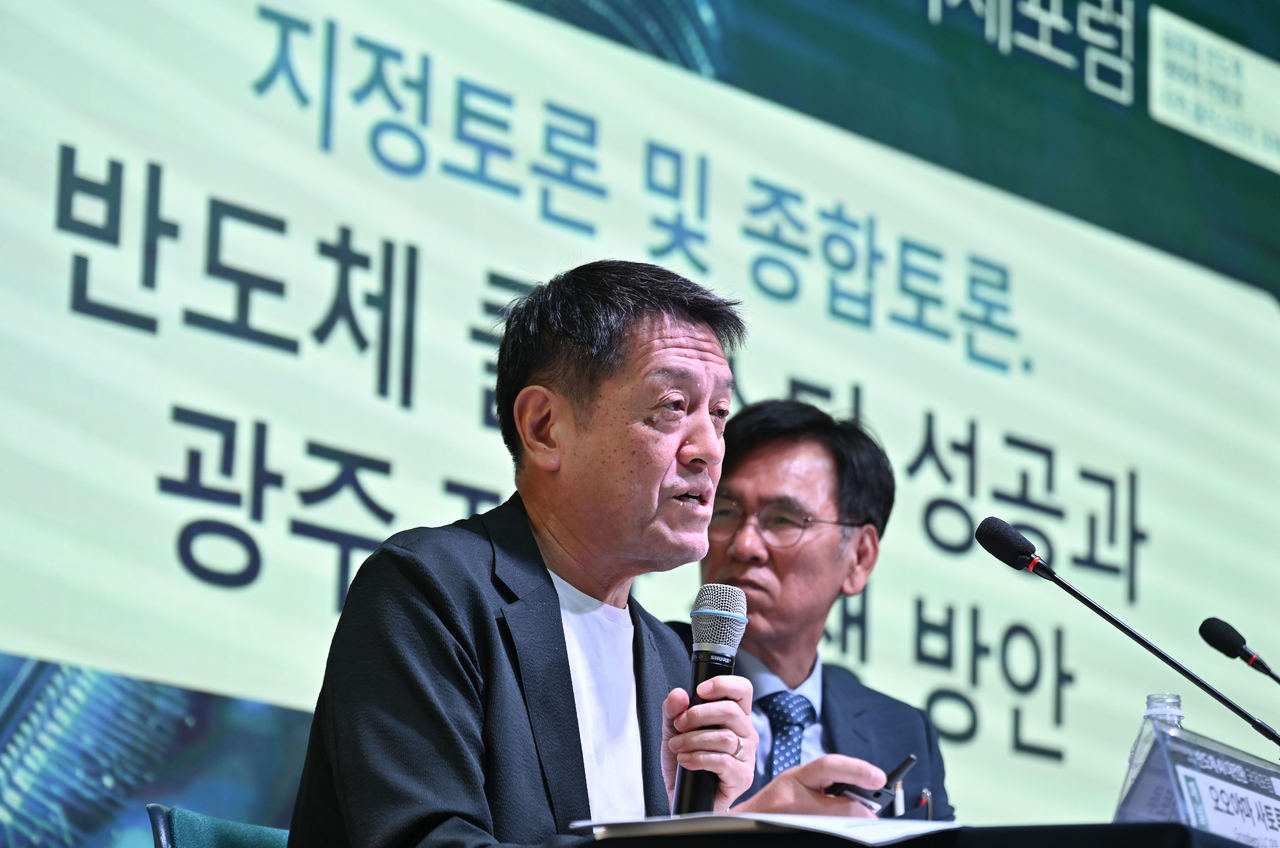
In the panel discussion that followed, Satoru Oyama, CEO of Grossberg LLC and a former management strategy executive in Fujitsu's semiconductor division, cited Japan's Kumamoto and Hokkaido cases to underscore the need for practical support measures.
As Japan's share of the global semiconductor market has continued to decline, the government has set a target of tripling semiconductor production value to 15 trillion yen ($97.1 billion) by 2030, compared with 2020 levels.
"There was a strong will to build a semiconductor cluster, and Kumamoto Prefecture devised a plan to provide funding and bring together related companies and organizations," Oyama said. "It was not just about attracting factories — the prefecture also built talent infrastructure that included high schools and universities."
He also suggested South Korea should focus more on its two leading memory chip makers. "In Japan, Kioxia is about the only company capable of investing in semiconductors," he said. "South Korea already has Samsung Electronics and SK hynix, so it is important to first look at what these companies need."
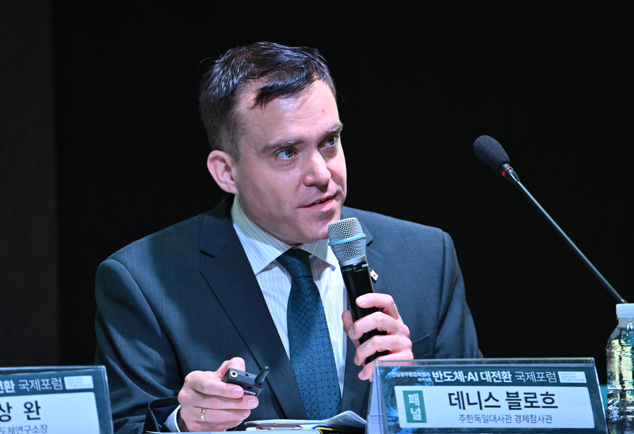
Dennis Bloch, economic counselor at the German Embassy in Seoul, introduced the case of "Silicon Saxony," formed in Dresden in the German state of Saxony. Built up since 1961, Silicon Saxony now plays a key role in Europe's semiconductor ecosystem, having drawn investment from Siemens, Infineon, AMD and TSMC. A third of all semiconductors produced in Europe are made there, he said.
"A semiconductor cluster is not built overnight — it takes decades," Bloch said. "Governments and politicians change, but what matters is the local community's commitment to staying the course."
Bloch attributed Silicon Saxony's success to the government's long-term support and investment in research and development, which enabled efficient networking. "More than 750 member companies can build constant cooperative networks within a single association," he said. "To provide skilled jobs, we also strengthened vocational training capacity so that about 2,000 people can be trained at once."
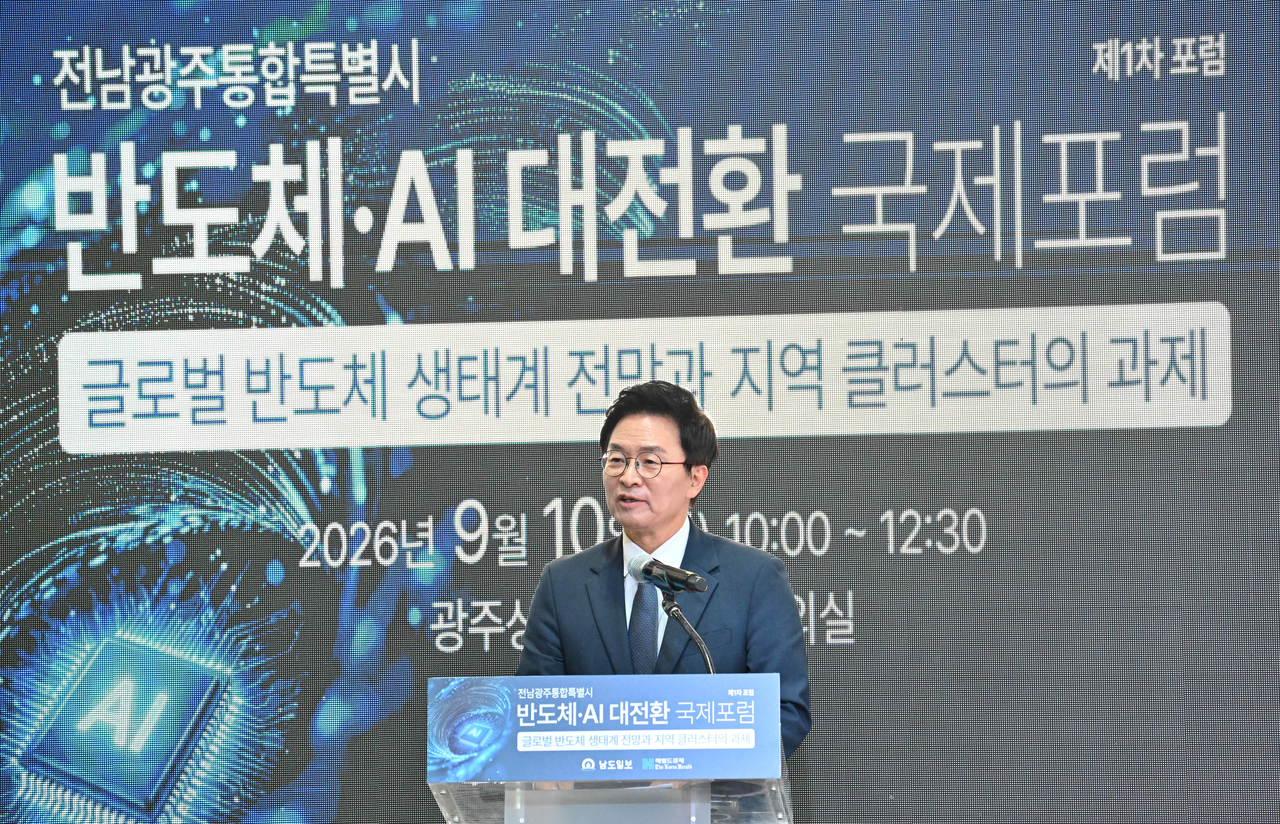
Some speakers also called for a long-term infrastructure expansion plan ahead of full-scale investment in the southwestern semiconductor cluster.
"The investment plan initially started with four fabs, but there is already talk of expanding to 11 fabs given projected chip demand," said Rep. Jung Jin-wook, a member of the National Assembly's Trade, Industry, Energy, SMEs and Startups Committee. "Rather than focusing only on the four fabs, I ask that water and power grid plans be drawn up with a long-term view of where new factories might be built a decade from now."
"In that sense, Gwangju needs to become a place where companies and people want to come and live," Jung said. "For Gwangju and South Jeolla Province to sustain themselves as a semiconductor hub, the city needs urban design and livability conditions that match that role."
The discussion also touched on the energy issue that has surfaced since the southwestern semiconductor cluster investment was first announced. Lee Soon-hyung, a professor at Dongshin University who has worked on large-scale power projects for more than 30 years, said that after the southwestern investment was announced, many participants at a meeting held at the Seoul Chamber of Commerce and Industry asked whether the Honam region could supply enough power. "We analyzed the Honam region's power grid and explained, with concrete data, that it is possible," he said.
He added that securing the 6.4 GW of power needed for the southwestern semiconductor cluster would require careful prioritization of power facility investment.
Ryu Sang-wan, director of Chonnam National University's Semiconductor Research Institute, focused on workforce and ecosystem development. "Even if a fab comes to our region, whether the people working there will actually be from the southwestern region is a separate matter," Ryu said. "If we neglect workforce training, it will not translate into jobs." He added that the same applies to materials, parts and equipment suppliers — most of which are concentrated in the greater Seoul area — and that the region must build competitiveness in that sector to avoid a situation where only the fab arrives.
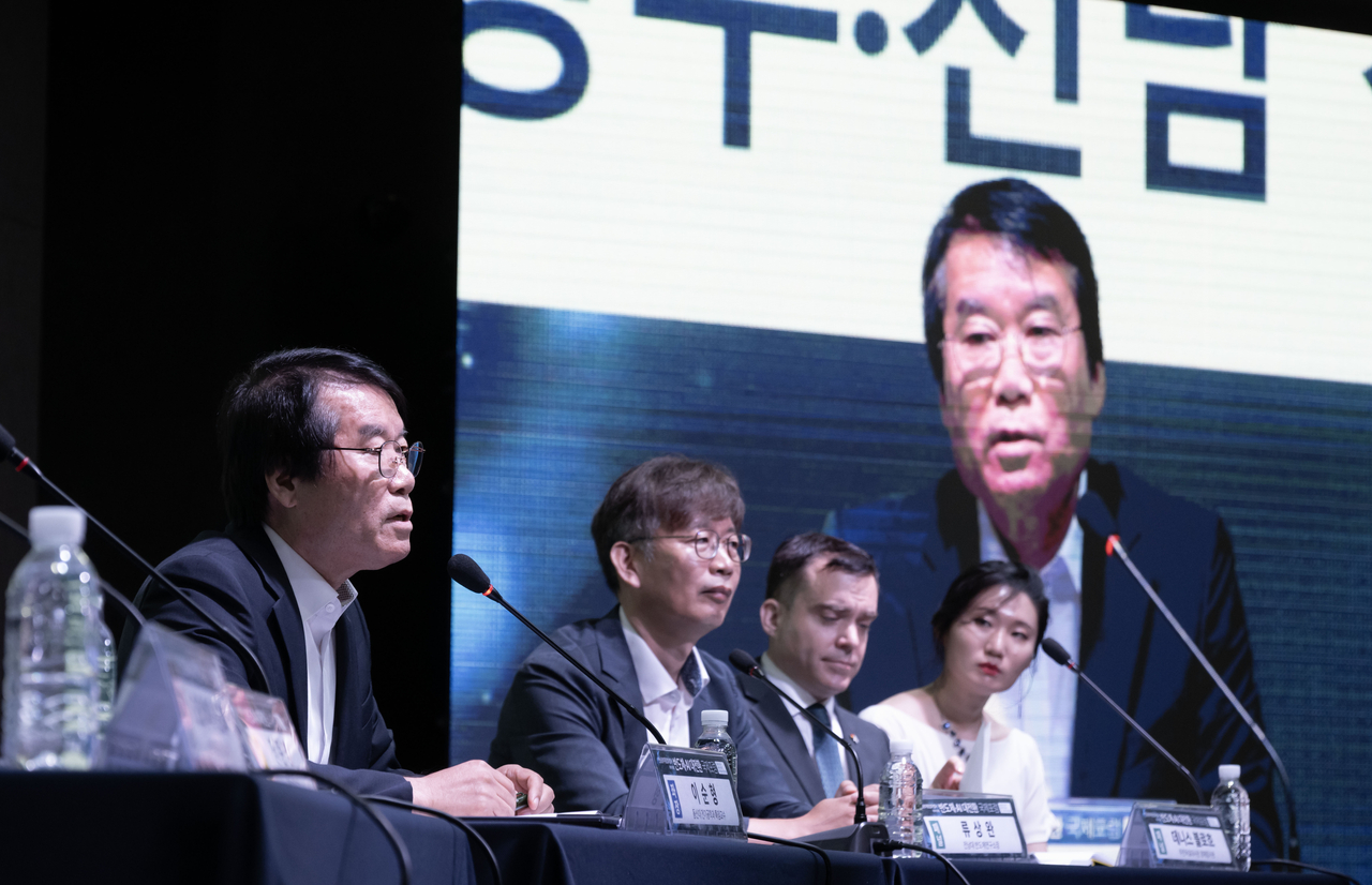
Meanwhile, Chung Eun-seung, chairman of the Jeolla-Gwangju Semiconductor Strategy Committee and a former chief technology officer of Samsung Electronics' Device Solutions division, stayed until the end of the forum, listening closely to the presentations and posing questions to the Japanese and German experts about their respective cases.
After the event, Chung said that while the background behind the Japanese and German semiconductor clusters discussed in Friday's session differed somewhat from that of the southwestern cluster, there was much to take away. "We will keep in mind the lessons we can learn," he said.
jeongwan@heraldcorp.com