Semiconductor substrate and packaging exhibition opens in Incheon's Songdo
Large-area substrate exceeding 100 millimeters per side debuts
Draws on 50 years of substrate expertise; mass production targeted for next year
Glass substrate technology for 2028 mass production also showcased
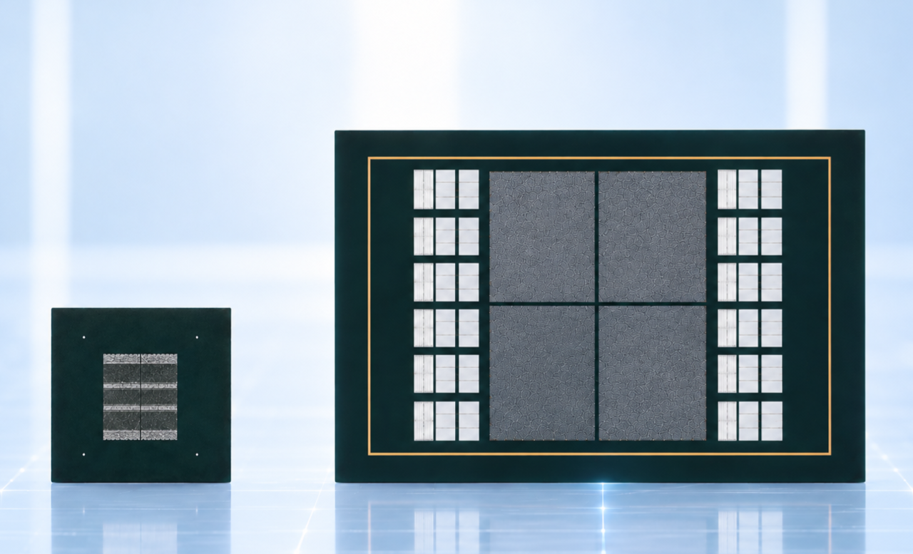
LG Innotek has unveiled a high-performance flip-chip ball grid array, or FC-BGA, substrate designed for AI accelerators for the first time.
The company said it is showcasing next-generation substrate technologies and products at KPCA Show 2026, the International PCB and Advanced Packaging Industry Exhibition. The event runs Wednesday through Friday at Songdo Convensia in Incheon.
Now in its 23rd year, KPCA Show is South Korea's largest exhibition dedicated to printed circuit boards and semiconductor packaging, hosted by the Korea Printed Circuit Association.
The FC-BGA substrate for AI accelerators, making its debut at the exhibition, is a high-spec semiconductor substrate that connects chips to mainboards.
Because it is used in high-performance chips such as GPUs and NPUs, the substrate requires higher circuit density and large-area design capabilities than conventional FC-BGA substrates.
The newly unveiled substrate is a large-area product measuring more than 100 millimeters per side. It draws on core technologies LG Innotek has built up over more than 50 years in the substrate business, including ultra-fine circuit implementation and high-layer-count design. The company aims to begin mass production next year.
At the exhibition, LG Innotek is presenting not only an 85-by-85-millimeter large-area FC-BGA substrate but also a sample of an even larger substrate, about 40 percent bigger in area.
The company is also introducing chip embedding technology, which underscores the differentiated competitiveness of its FC-BGA products. Unlike the conventional method of mounting chips on the substrate's surface, this technology places chips inside the substrate itself, minimizing the connection distance between chip and substrate. This improves signal transmission performance while lowering electrical resistance, reducing power loss.
LG Innotek is also showcasing glass substrate technology, which is drawing attention as a next-generation packaging solution optimized for FC-BGA. Glass substrates replace the core layer inside the substrate with glass, minimizing warping and circuit distortion. The company is accelerating development of the technology with a target of mass production in 2028.
"At this exhibition, visitors will be able to see intuitively how LG Innotek's substrates are used across industries and everyday life, from AI and smartphones to mobility," said Cho Ji-tae, executive vice president and head of the company's package solution business division. "We will lead innovation to change the paradigm of the substrate market."
Meanwhile, LG Innotek's package solution business posted sales of 935.6 billion won ($697 million) and operating profit of 99.6 billion won in the first half of this year. That marked increases of 18 percent and 94 percent, respectively, from a year earlier. Its operating margin also rose from 6.5 percent to 10.6 percent, demonstrating both growth and profitability.
LG Innotek has designated the package solution business as a key future growth driver, aiming to raise its operating profit to 1 trillion won by 2031.
jeongwan@heraldcorp.com