![President Lee Jae Myung raises a toast with attendees at a Global AI Leaders Dinner held at The Ramp Restaurant in San Francisco on Friday (local time). From left: Lee Hae-jin, chairman of Naver's board of directors; Chey Tae-won, chairman of SK Group; Ranie Borkar, corporate vice president of Microsoft Azure Hardware; Jensen Huang, CEO of Nvidia; President Lee Jae Myung; Hock Tan, CEO of Broadcom; Lee Jae-yong, chairman of Samsung Electronics; and Euisun Chung, chairman of Hyundai Motor Group. [Joint press corps]](https://wimg.heraldcorp.com/news/cms/2026/07/25/rcv.YNA.20260725.PYH2026072503520001300_P1.jpg)
Samsung Electronics announced it will enter into a strategic collaboration with global semiconductor design firm Broadcom worth $200 billion through 2030, spanning memory chips, foundry and packaging.
Samsung signed a strategic MOU with Broadcom at the "AI Summit" held at The Midway in San Francisco on Friday (local time), aimed at building next-generation AI core infrastructure. Han Jin-man, president and head of Samsung's foundry division, and Broadcom CEO Hock Tan attended alongside executives from both companies and government officials.
The agreement is a strategic partnership to deepen cooperation across memory chips, foundry and advanced packaging — the key semiconductor technologies of the AI era — and to strengthen the competitiveness of the next-generation AI semiconductor ecosystem.
"Based on our world-exclusive one-stop turnkey solution encompassing memory chips, foundry and advanced packaging, we plan to expand cooperation with Broadcom and deliver differentiated customer value in the next-generation AI semiconductor market," a Samsung Electronics official said. The MOU ranks among the largest single-company agreements Samsung has signed.
Collaboration extends beyond HBM4 to foundry and packaging
Samsung to manufacture Broadcom ASICs on 2-nanometer process
Cutting-edge memory chip solutions including HBM to continue flowing
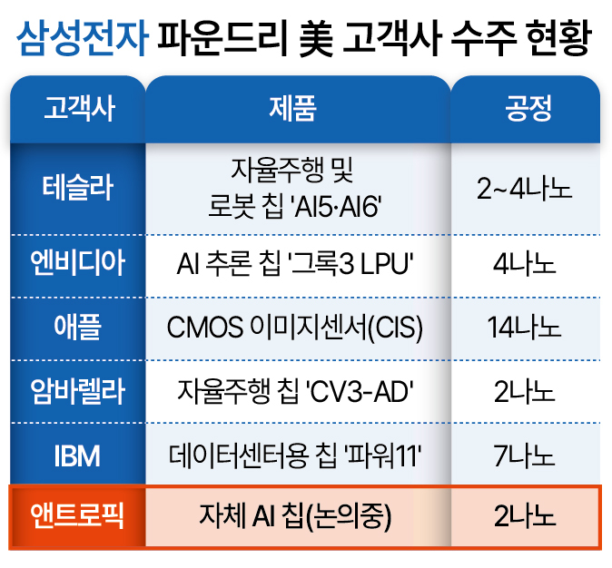
The MOU signals recognition of Samsung Electronics' competitiveness in the ASIC (application-specific integrated circuit) space, and analysts say it gives fresh momentum to Samsung's foundry business. Global big-tech companies have been rapidly accelerating adoption of their own AI accelerators based on ASICs. Under the agreement, Samsung and Broadcom will broaden their cooperation well beyond memory chips to encompass manufacturing and packaging technology.
Samsung will supply HBM (high-bandwidth memory) and other cutting-edge memory chip solutions, drawing on its world-class memory technology and commanding competitive edge, to help boost the performance and competitiveness of Broadcom's AI accelerators.
Last February, Samsung became the first in the industry to begin mass production and shipment of HBM4 incorporating 1c DRAM and a 4-nanometer base-die technology. In May it was again first to supply samples of HBM4E — the next generation of HBM — to customers, reclaiming its leadership in HBM technology.
Samsung's HBM is set to serve as a core memory chip solution underpinning next-generation AI infrastructure, maximizing the performance of Broadcom's AI accelerators through industry-leading performance, reliability and power efficiency.
The extension of the collaboration into foundry is particularly significant. Samsung will apply its most advanced sub-2-nanometer foundry process to key product lines for Broadcom, including semiconductor solutions for high-speed data communications, further sharpening their competitiveness.
Samsung will also support the development of high-performance, high-efficiency AI semiconductors through advanced packaging technology based on its 2-nanometer process, delivering differentiated AI semiconductor solutions to Broadcom.
In addition, Samsung will provide support across the entire development cycle — from the co-optimization of chip design and manufacturing processes through chip design, advanced packaging and mass production — to shorten product development timelines and maximize performance and power efficiency.
Building on this technological competitiveness, Samsung plans to continue expanding its cooperation with Broadcom in next-generation AI semiconductors and to actively pursue new business opportunities in the fast-growing AI and high-performance computing market.
"In the AI era, tightly integrated semiconductor solutions combining memory chips, logic and advanced packaging are critical," said Jun Young-hyun, Samsung Electronics CEO and head of the DS division. "By expanding our cooperation with Broadcom, we will accelerate the development of future AI infrastructure and deliver greater value to our customers."
go@heraldcorp.com