Samsung Electronics Chairman Lee Jae-yong visited a newly established advanced packaging research lab in Yokohama on the company's 57th founding anniversary, signaling his drive to extend Samsung's dominance beyond memory chips into next-generation packaging technology as the AI era reshapes the semiconductor landscape.
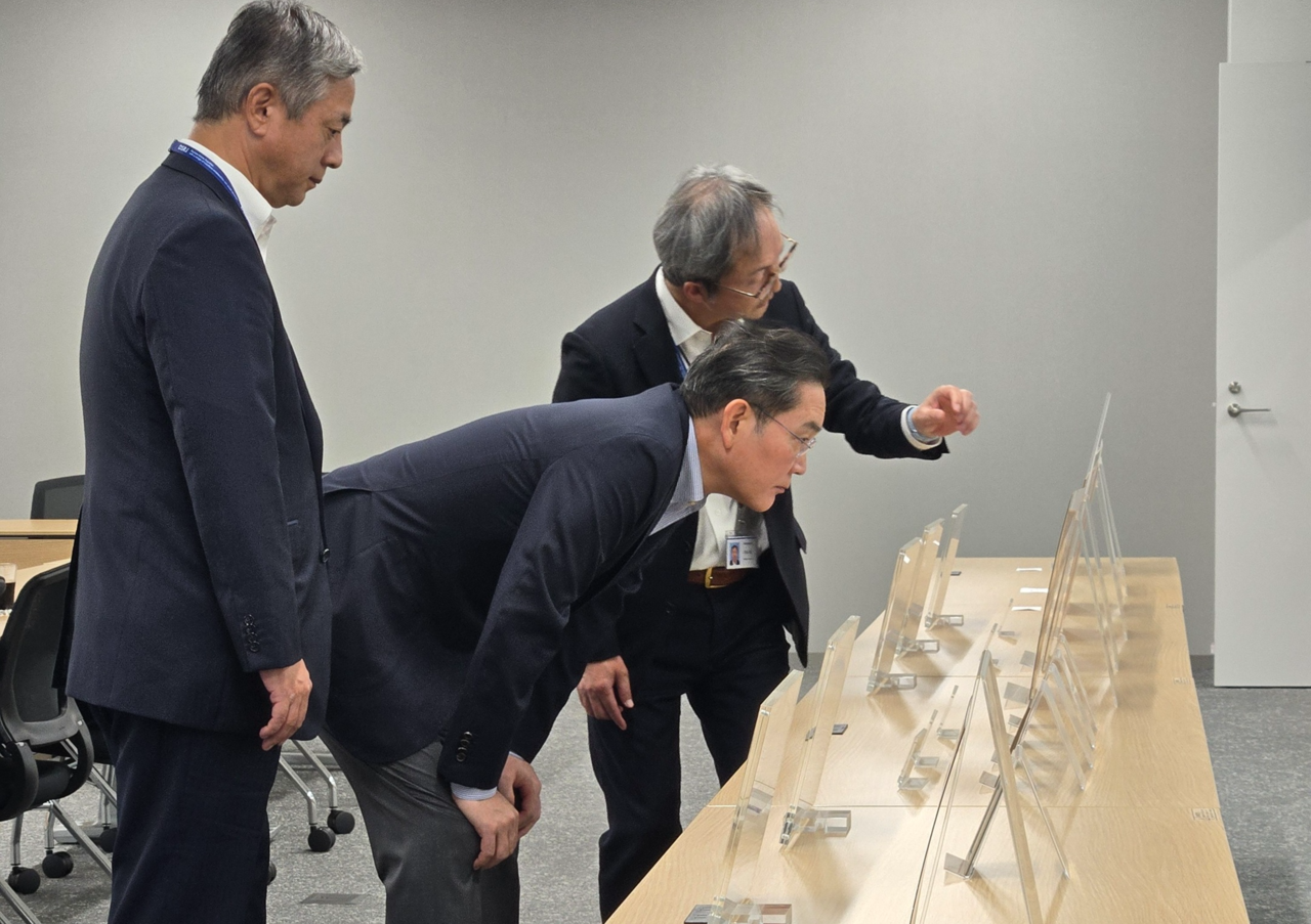
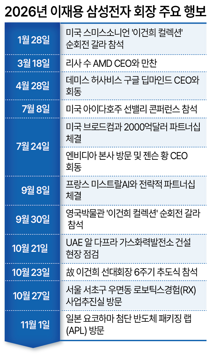
Samsung Electronics Chairman Lee Jae-yong is making a series of on-site visits to assess the company's readiness in next-generation technologies that will shape its future competitiveness.
Lee, who has long championed what he calls "fundamental technological competitiveness," has been moving briskly between domestic and overseas sites in a push to reinforce Samsung's identity as a technology leader.
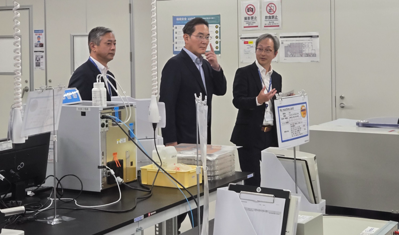
On Sunday — Samsung Electronics' 57th founding anniversary — Lee visited the Advanced Package Lab (APL), the company's advanced semiconductor packaging research hub in Yokohama, Japan, to review progress on next-generation packaging component technologies, the company said Monday.
The visit came as Samsung's memory chip business posted a record 106.5 trillion won ($79.8 billion) in operating profit from semiconductors alone in the third quarter, and as advanced packaging emerges as a new battleground in the AI era.
The semiconductor industry has identified advanced packaging — the process of assembling multiple chips such as CPUs, GPUs and HBM onto a single substrate — as a critical technology for boosting AI chip performance.
The APL, which opened Sept. 8, develops and validates component technologies — including materials and processes — needed for advanced semiconductor packaging. The lab has its sights set on a range of next-generation technologies such as wafer bonding and glass substrates, as well as new packaging architectures for mass-producing low-power, high-performance AI chips.
Through the Yokohama visit, Lee signaled determination to achieve a decisive lead in advanced packaging technology — a key pillar of future competitiveness — just as Samsung has sought to do in memory and logic chips.
Japan, home to many of Samsung's semiconductor materials, components and equipment partners, is a frequent destination for Lee. Samsung maintains regular meetings with member companies of LJF (Lee Kunhee Japanese Friends), a network of the company's Japanese partners.
Samsung Electronics has been building its research and development base in Japan with an investment of 40 billion yen ($254 million) over five years starting in 2024. The APL serves as a bridge between Samsung's semiconductor design and manufacturing capabilities and Japan's strong ecosystem of materials, components and equipment technology.
Lee has also been directing attention to robotics, another business Samsung is cultivating as a future core operation. On Tuesday — the fourth anniversary of Lee's appointment as chairman — Lee visited the Robotics Experience (RX) Business Promotion Office at Samsung's Seoul R&D Campus in Umyeon-dong, Seocho-gu, Seoul.
The RX office and the Yokohama APL share a common thread: both are newly established units — opened in July and September, respectively — and both are positioned as forward bases for identifying Samsung's next engines of growth.
Lee plans to steadily expand the local research workforce at the APL and develop Yokohama into a global hub for next-generation packaging component technology.
Alongside its future technology research, Samsung is accelerating an internal AI transformation drive. As part of that effort, the company invited OpenAI CEO Sam Altman to Samsung Human Resources Development Center in Yongin, Gyeonggi Province, on Friday for a roundtable with about 50 affiliate presidents on the theme "The next decade AI will change — choices for companies."
Samsung has staked its future on embedding AI across every function — from research and development to production, marketing and support — to lift workforce productivity and sharpen business competitiveness. To that end, the company has pushed its top executives to deepen their understanding of AI and incorporate it into their decision-making.
joze@heraldcorp.com